Critical PCB Design for Industrial Control: Solutions for High-Temperature & Anti-Interference Performance
- afax TE.
- Jan 10
- 4 min read
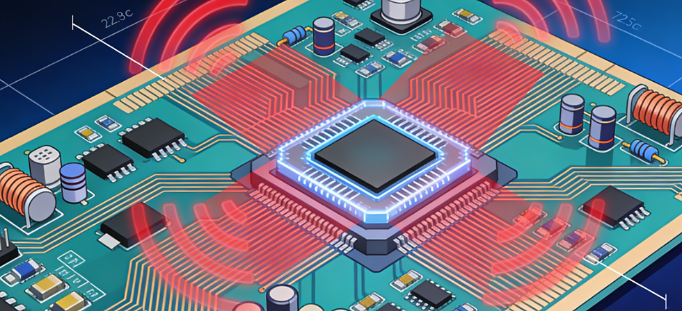
In the demanding world of industrial automation and control, the reliability of the hardware is non-negotiable. From factory floors to energy substations, Printed Circuit Boards (PCBs) are the central nervous system of control equipment, operating in environments fraught with thermal stress and electromagnetic chaos. A standard commercial-grade PCB design is destined to fail under such conditions. This guide delves into the critical PCB design solutions for industrial control systems, focusing specifically on the essential pillars of reliability: high-temperature endurance and robust anti-interference capabilities.
Introduction: Why Industrial PCB Design is a Unique Challenge
Industrial control equipment—encompassing PLCs, motor drives, DCS modules, and remote I/O units—must perform with unwavering precision for years, often decades. The core challenges are:
Thermal Stress: Heat from high-power components, dense packaging, and elevated ambient temperatures can degrade materials and cause premature failure.
Electromagnetic Interference (EMI): A noisy environment filled with variable-frequency drives, heavy motors, power lines, and wireless signals can disrupt sensitive analog and digital signals, leading to data corruption, false triggering, and system crashes.
Addressing these challenges at the PCB design stage is the most cost-effective and reliable strategy, preventing field failures and costly recalls.
Part 1: High-Temperature Endurance: Designing for Thermal Resilience
Thermal management in PCB design is not just about adding a heatsink; it's about creating a foundation that can withstand sustained thermal cycling and high ambient temperatures.
1. Material Selection: The First Line of Defense
High-Tg (Glass Transition Temperature) Laminates: Standard FR-4 (Tg ~130-140°C) can soften and delaminate in hot environments. Opt for high-Tg FR-4 (Tg > 170°C) or advanced materials like Polyimide (Tg > 250°C) for the most demanding applications. These materials maintain mechanical and electrical stability at elevated temperatures.
Thermal-Conductive Dielectrics: For boards with concentrated heat sources (e.g., power regulators), consider substrates with ceramic fillers (e.g., metal-core PCBs or insulated metal substrates). These materials efficiently conduct heat away from critical components to a heatsink or the board's edge.

2. Layout & Copper Design for Heat Dissipation
Thermal Vias & Planes: Strategically place arrays of thermal vias directly under or near high-power components (e.g., MOSFETs, converters). These vias conduct heat from the top layer to internal ground/power planes or a bottom-side heatsink layer. Filling these vias with thermally conductive epoxy further enhances performance.
Copper Pour and Thickness: Use generous copper pours (connected to appropriate nets) on outer and inner layers to act as heat spreaders. Increasing copper weight (e.g., from 1oz to 2oz) for high-current traces and planes significantly improves current handling and thermal dissipation.
Component Placement & Spacing: Avoid clustering high-heat components. Distribute them across the board to prevent creating localized hot spots. Ensure adequate airflow space as per the mechanical enclosure design.
3. Manufacturing & Assembly Considerations
High-Temperature Solders: Specify lead-free solders with higher melting points (e.g., SAC305) for assemblies that will experience sustained high operating temperatures.
Conformal Coating: Apply high-performance conformal coatings (e.g., acrylic, silicone, or polyurethane) to protect the assembled board from moisture, dust, and chemical contaminants, which can exacerbate failure under thermal stress.

Part 2: Anti-Interference Design: Ensuring Signal Integrity in a Noisy Arena
Electromagnetic Compatibility (EMC) is paramount. Your PCB must neither be susceptible to external noise nor become a source of it.
1. Grounding: The Foundation of Clean Signals
Strategic Partitioning: Divide the board into clear functional zones: analog, digital, power, and RF. Implement a segmented ground plane strategy, connecting these ground regions at a single, low-inductance point (usually the power supply input) to prevent noisy return currents from contaminating sensitive circuits.
Solid Ground Planes: Use at least one continuous, unbroken layer as a dedicated ground plane. This provides the lowest-impedance return path for signals, minimizing ground bounce and acting as a shield against EMI.
2. Power Integrity: A Stable Foundation
Comprehensive Decoupling: Place a mix of bulk (electrolytic/tantalum) and high-frequency (ceramic) decoupling capacitors as close as possible to the power pins of every IC. Follow the manufacturer's guidelines meticulously. This creates a local reservoir of charge, suppressing high-frequency noise on the power rails.
Power Plane Design: Utilize dedicated power planes where possible. If using power traces, ensure they are wide enough for current capacity and are closely coupled to their corresponding ground plane to reduce loop area and inductance.

3. Routing & Layout for EMI Reduction
Controlled Impedance Routing: For high-speed signals (clocks, differential pairs, data buses), calculate and route them as controlled impedance lines. This prevents signal reflections and crosstalk, which are sources of internal EMI.
Minimizing Loop Areas: The area between a signal trace and its return current path acts as an antenna. Keep high-speed or high-current traces close to their reference ground plane to minimize this loop area, drastically reducing both emissions and susceptibility.
Shielding & Guarding: For extremely sensitive circuits (e.g., high-gain sensor inputs), use guard traces (grounded copper traces surrounding the signal) or even on-board shielding cans to isolate them from noise sources.
4. Filtering & Isolation at Interfaces
Ferrite Beads & Common-Mode Chokes: Use these on all cable entry/exit points (power, communication lines) to suppress high-frequency common-mode noise.
Galvanic Isolation: For communication ports (RS-485, Ethernet) or sensor inputs exposed to harsh external environments, integrate optocouplers or digital isolators. This creates a physical break in the ground path, preventing ground loops and protecting the core logic from surges and transients.

Conclusion: An Integrated Approach to Reliability
In industrial control PCB design, high-temperature resilience and anti-interference robustness are not isolated tasks—they are deeply interconnected design philosophies. A board that dissipates heat well will have more stable electrical characteristics. A board with impeccable EMC design will inherently have lower noise-related thermal stress on components.
Successful design requires forethought, discipline in layout, and collaboration with a PCB manufacturer experienced in industrial-grade materials and processes. By implementing these critical solutions from the initial design phase, you build more than just a circuit; you build the unwavering reliability that industrial applications demand. Ready to engineer unparalleled reliability into your industrial control system? Our team specializes in high-temperature, high-interference PCB design and manufacturing. If you have specific procurement intentions or need further assistance, please feel free to contact us at sales03@sunsoartech.com or call +8613632793113.


Comments