5 Critical Attributes of a High Reliability PCB: From Material Selection to Surface Finish
- afax TE.
- Jan 14
- 3 min read
Introduction
In industries where failure is not an option—such as aerospace, medical devices, automotive, and industrial control—standard PCBs are insufficient.
High reliability PCBs are engineered to endure extreme stresses, maintain stable performance over long lifetimes, and ensure zero-defect operation.True reliability is not achieved by a single step but is built into the board through a meticulous, full-process approach. This article breaks down the five fundamental pillars that define a high-reliability printed circuit board.

1. Foundation: Advanced PCB Material Selection
The journey to reliability begins at the substrate level. Material choice dictates thermal, mechanical, and electrical performance under stress.
High-Tg FR-4: For elevated temperature environments, standard FR-4 is inadequate. High Glass Transition (Tg) materials (Tg > 170°C) resist softening, preventing delamination and maintaining mechanical integrity during thermal cycling.
Low-Loss Laminates: For high-speed or RF applications, materials with low dielectric constant (Dk) and dissipation factor (Df) minimize signal loss, distortion, and crosstalk, ensuring signal integrity.
Specialty Materials: Applications with extreme demands utilize polyimide (for superior flex endurance), PTFE/Rogers (for high-frequency performance), or metal-core boards (for exceptional thermal management).
Our Expertise: We guide clients through material trade-offs (cost vs. performance), selecting the optimal laminate that meets specific thermal, electrical, and environmental requirements.

2. Precision Engineering: Design for Manufacturability (DFM) & Reliability (DFR)
A perfect design on screen must translate into a manufacturable, robust board. DFM/DFR bridges this gap.
Controlled Impedance: Careful stack-up design and trace geometry calculation ensure impedance matching, critical for signal integrity in high-speed designs.
Thermal Management: Incorporating thermal reliefs, adequate copper balancing, and strategic via placement prevents hotspots and manages heat dissipation.
Stress Reduction: Avoiding acute angles, using tear reliefs for connectors, and defining proper pad sizes minimize mechanical and thermal stress points that can lead to cracks.
Our Process: Our engineers conduct a thorough DFM/DFR analysis on every design, providing actionable feedback to eliminate failure points before fabrication begins.

3. Manufacturing Excellence: Tight Process Control & Standards
Consistency is the hallmark of reliability. This demands adherence to the highest industry standards and rigorous process control.
Certifications & Standards: Compliance with IPC-A-600 (Acceptability of PCBs) and IPC-6012 (Performance Specification for Rigid PCBs) Class 2 or 3 is the baseline for high-reliability boards.
Process Control: Utilizing Automated Optical Inspection (AOI), Electrical Testing (Flying Probe/Test Fixture), and Controlled Impedance Testing at critical stages ensures every board meets specification.
Our Commitment: We operate certified manufacturing lines with documented process controls, providing full test reports and traceability for every batch.

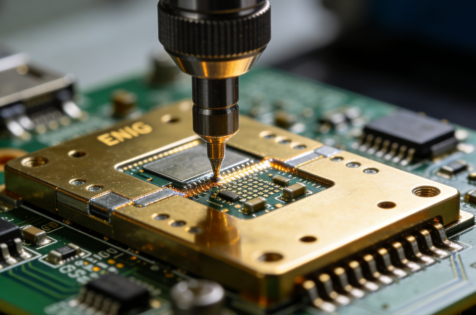
4. The Critical Interface: PCB Surface Finish Selection
The surface finish protects exposed copper from oxidation and ensures a solderable, reliable surface for component assembly. The choice significantly impacts solder joint strength, shelf life, and performance.
ENIG (Electroless Nickel Immersion Gold): The industry standard for high reliability. Offers a flat surface for fine-pitch components, excellent oxidation resistance, and good solderability. Nickel acts as a robust barrier layer.
ENEPIG (Electroless Nickel Electroless Palladium Immersion Gold): Superior for gold wire bonding and demanding applications. The palladium layer prevents "black pad" syndrome and provides exceptional durability.
Immersion Silver/Tin: Cost-effective alternatives with good solderability, but require careful handling due to susceptibility to tarnishing (Ag) or whisker growth (Sn).
Our Recommendation: We analyze your assembly process, component types, and end-use environment to recommend the optimal surface finish—often ENIG or ENEPIG—that guarantees long-term solder joint integrity.
5. Validation & Testing: Proving Reliability
The final step is validation through stringent testing that simulates real-world operating life and stress conditions.
Accelerated Life Testing: Thermal Cycling and H.A.S.T. (Highly Accelerated Stress Test) expose material and plating weaknesses by rapidly aging the board.
Solderability Testing: Ensures the surface finish will form perfect solder joints during assembly, even after storage.
Ionic Contamination Testing: Verifies the cleaning process removes all flux residues that could lead to electrochemical migration and corrosion.
Our Validation Suite: We offer a full range of reliability testing services to provide the data and confidence that your boards will perform as specified in their operational lifecycle.

Conclusion
A high-reliability PCB is the product of intentional choices at every stage—from the molecular structure of its base material to the final validation of its surface. It is a synergy of science, engineering, and uncompromising process control.By mastering these five key attributes—Material Selection, DFM/DFR, Process Control, Surface Finish, and Rigorous Testing—we deliver not just a board, but a foundation of trust for your most critical electronic systems.
Partner with a manufacturer that builds reliability in, not tests it out. Contact us today to discuss the specifications for your next high-reliability PCB project.
If you have specific procurement intentions or need further assistance, please feel free to contact us at sales03@sunsoartech.com or call +8613632793113.


Comments