5 Key Performance Advantages of HDI PCBA Over Traditional Circuit Boards
- afax TE.
- Dec 23, 2025
- 3 min read
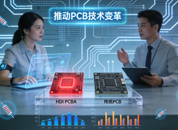
For engineers and procurement specialists pushing the boundaries of electronics, the quest for higher performance in smaller, more reliable packages is relentless. This drive is fundamentally reshaping printed circuit board (PCB) technology. High-Density Interconnect (HDI) PCBA has emerged as the superior solution, outperforming traditional PCB designs across critical parameters. Here, we analyze the five key performance advantages that make HDI the cornerstone of advanced electronic design.

1. Superior Miniaturization with Enhanced Functionality
The most apparent benefit of high-density PCBA design is its revolutionary space efficiency. HDI technology utilizes finer lines, micro-vias (including blind and buried vias), and higher connection pad densities. This allows for the placement of more components on both sides of the board and in multiple layers within a drastically reduced footprint.
Performance Impact: Enables the development of ultra-compact, lightweight devices—from sophisticated medical implants and wearable tech to advanced avionics and military communications equipment—without sacrificing functional complexity. This directly translates to product innovation and competitive edge.

2. Enhanced Electrical Performance and Signal Integrity
As signal speeds skyrocket, managing integrity becomes paramount. The compact architecture of HDI boards provides shorter signal paths between components. This reduction in interconnect distance decreases propagation delay, capacitance, and inductance.
Performance Impact: Results in faster signal transmission speeds, reduced cross-talk, and improved overall signal integrity. This is a critical HDI PCBA performance advantage for high-speed applications like networking hardware, high-frequency RF systems, and cutting-edge data processors, ensuring stable and reliable operation.

3. Unmatched Reliability and Robustness
HDI PCBA performance advantages extend deeply into reliability. The use of advanced micro-via structures—particularly laser-drilled vias—creates more robust connections than traditional through-hole vias. The higher interconnection density also allows for better power distribution and thermal management across the board.
Performance Impact: Fewer potential failure points, improved thermal dissipation, and greater resistance to thermal stress and physical shock. This leads to higher mean time between failures (MTBF), a crucial metric for automotive, aerospace, and industrial applications where failure is not an option.
4. Greater Design Flexibility and Integration Potential
High-density PCBA design benefits empower engineers with unprecedented freedom. The ability to place components closer together and utilize sequential lamination processes allows for more innovative and efficient layouts. This facilitates the integration of complex technologies like fine-pitch Ball Grid Array (BGA) and Chip-Scale Package (CSP) components.
Performance Impact: Engineers can optimize circuit pathways for both performance and manufacturability. This flexibility accelerates innovation, supports system-in-package (SiP) designs, and enables the integration of analog, digital, and RF functions into a single, high-performance module.

5. Long-Term Cost Efficiency and Value
While the initial cost per board may be higher, the total cost of ownership for HDI PCBA often proves lower. The miniaturization reduces raw material usage (smaller board size, fewer layers for equivalent functionality). More significantly, the enhanced reliability reduces warranty claims and field failures.
Performance Impact: Higher yield rates in complex assemblies, lower long-term maintenance costs, and a superior end-product that commands a market premium. For procurement, this means better value and lower total lifecycle cost, justifying the investment in advanced HDI technology.
Conclusion: The Clear Choice for Advanced Electronics
The transition from traditional PCBs to HDI PCBA is not merely an incremental step; it's a strategic leap towards superior performance, reliability, and innovation. The combined advantages of HDI PCBA—miniaturization, enhanced electrical properties, robust reliability, design freedom, and lifecycle value—make it the indispensable technology for next-generation electronics.

Is your current design constrained by the limitations of traditional boards? Are you seeking a manufacturing partner with deep expertise in high-density PCBA design to unlock these performance advantages for your product?
Explore our advanced PCBA capabilities and contact our engineering team today to discuss how we can optimize your next high-performance project.
If you have specific procurement intentions or need further assistance, please feel free to contact us at sales03@sunsoartech.com or call +8613632793113.


Comments