7 Common PCBA Soldering Defects: Causes and Prevention Strategies
- afax TE.
- Dec 30, 2025
- 4 min read
Soldering defects are among the most frequent challenges in PCBA manufacturing, directly impacting product reliability, yield rates, and overall cost. For procurement specialists and engineers grappling with quality control issues, understanding the root causes of these defects is the first step toward robust prevention. This technical analysis details seven common PCBA soldering defects, explores their underlying causes, and provides actionable preventive measures to enhance your assembly quality.

1. Solder Bridging (Short Circuits)
Description: Unintended solder connections between two adjacent pins or conductors, creating an electrical short.
Root Causes:
Excessive Solder Paste: Due to over-printed paste, a damaged stencil, or incorrect stencil aperture design.
Insufficient Solder Mask between tight-pitch components.
Incorrect Reflow Profile, causing excessive paste flow before wetting.
Poor Component Placement alignment.
Prevention Strategies:
Optimize stencil design with appropriate aperture size and shape (e.g., nano-coating, trapezoidal walls).
Strictly control solder paste printing process and implement regular stencil cleaning.
Fine-tune the reflow oven temperature profile, particularly the ramp-up rate and peak temperature.
Ensure precision in component placement equipment calibration.

2. Tombstoning (Manhattan Effect)
Description: A passive component (like a chip resistor or capacitor) stands up vertically on one of its terminations.
Root Causes:
Uneven heating during reflow, causing one end to wet and solidify before the other.
Imbalanced solder paste volume or land size on the two component terminations.
Misaligned component placement.
Different thermal mass connections at each pad.
Prevention Strategies:
Design symmetric PCB pads with equal size and thermal relief.
Ensure uniform solder paste deposition on both pads.
Optimize the reflow profile for a balanced, gradual heating across the board.
Correctly align components during placement.
3. Voiding (in Solder Joints, especially BGA)
Description: Small cavities or pores trapped within the solder joint, often observed in X-ray images.
Root Causes:
Outgassing from flux volatiles or moisture trapped during the reflow process.
Contamination on pads or component leads (oxides, oils).
Insufficient reflow temperature or time.
Poor solder paste quality or improper handling (e.g., absorbed moisture).

Prevention Strategies:
Implement proper PCB and component baking procedures to remove moisture.
Use high-quality solder paste with appropriate flux chemistry and ensure proper storage.
Optimize the reflow profile, ensuring adequate time above liquidus for gases to escape.
Maintain impeccable cleanliness of PCB surfaces prior to assembly.
4. Cold Solder Joints
Description: A dull, grainy, or lumpy-looking joint with poor mechanical strength and unreliable electrical connection.
Root Causes:
Insufficient heat during the soldering process, preventing proper wetting.
Excessive movement or vibration of the joint before the solder has solidified.
Contaminated surfaces preventing proper metallurgical bonding.
Prevention Strategies:
Calibrate soldering equipment (irons, reflow ovens) to deliver consistent, adequate heat.
Ensure the thermal profile reaches the necessary peak temperature and time above liquidus.
Avoid any board movement during the cooling phase of reflow or hand soldering.
Enforce strict surface preparation and cleanliness protocols.
5. Solder Balling
Description: Small spheres of solder scattered around the joint or on the PCB surface.
Root Causes:
Oxidized solder paste or use of paste beyond its shelf life.
Too rapid heating during reflow, causing solder paste to splatter.
Excessive moisture in the solder paste or on the PCB.
Incorrect reflow atmosphere (inadequate nitrogen in the oven).
Prevention Strategies:
Adhere to solder paste handling and "first-in, first-out" inventory rules.
Use a reflow profile with a controlled preheat/soak stage to gently volatilize flux solvents.
Bake PCBs and components if moisture exposure is suspected.
Consider using a nitrogen-inerted reflow environment for fine-pitch or low-residue applications.

6. Insufficient Solder (Non-Wetting)
Description: The solder fails to flow properly onto the pad or component lead, resulting in a weak or incomplete joint.
Root Causes:
Low soldering temperature.
Poor solderability of the pad or component termination (oxidation, contamination).
Inadequate solder paste volume due to stencil clogging or poor printing.
Excessively short contact time with the soldering iron.
Prevention Strategies:
Verify and control the solderability of incoming PCBs and components.
Optimize solder paste printing to ensure sufficient deposit volume.
Adjust process parameters (temperature, time, pressure) to ensure proper heat transfer.
For hand soldering, use appropriately sized and tinned tips.
7. Lifted Pads
Description: The copper pad separates from the PCB laminate, often lifting with the component lead.
Root Causes:
Excessive mechanical stress during soldering, repair, or trimming.
Overheating during soldering or desoldering, damaging the pad adhesion.
Poor intrinsic adhesion of the pad to the substrate due to PCB manufacturing flaws.
Repeated rework on the same joint.
Prevention Strategies:
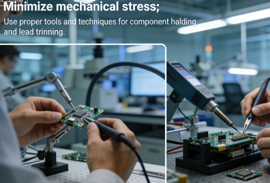
Minimize mechanical stress; use proper tools and techniques for component handling and lead trimming.
Apply controlled heat during all operations. Use thermal relief pads in design for multilayer boards.
Source PCBs from qualified manufacturers with strict quality control.
Limit the number of rework cycles on a single joint.
Conclusion: Building a Proactive Defense
Understanding the "why" behind soldering defects transforms quality control from reactive inspection to proactive prevention. The most effective strategy integrates Design for Manufacturability (DFM), meticulous material control, precise process parameter optimization, and continuous operator training.
By addressing these root causes, you can significantly reduce defects, improve first-pass yield, and build more reliable electronic products. For teams facing persistent or complex soldering issues, partnering with a PCBA manufacturer that masters these analytical and preventive practices is a critical step toward seamless production.
If you have specific procurement intentions or need further assistance, please feel free to contact us at sales03@sunsoartech.com or call +8613632793113.


Comments