From Concept to Connection: How PCB Design Shapes IoT Performance
- SUNSOAR TE.
- Jun 6, 2025
- 3 min read
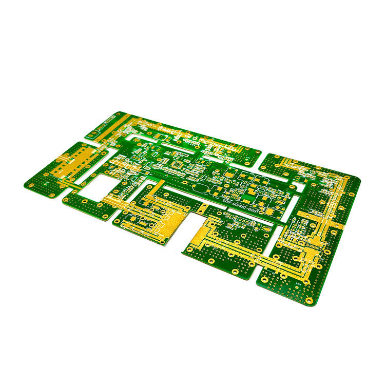
In the IoT world, every connected device must perform three fundamental tasks: sense, compute, and communicate. Whether it’s a smart door sensor or an industrial gateway, the quality and efficiency of these tasks depend not just on components, but on how they are integrated—through the printed circuit board (PCB).
For product designers and engineers, understanding the relationship between PCB design and overall IoT performance is not optional. It’s the difference between a device that simply works and one that works efficiently, reliably, and cost-effectively.
1. Design Starts with System-Level Thinking
🎯 Mapping Functional Requirements to Layout
Before even opening a CAD tool, the first step in IoT PCB design is translating your product's functional needs into a physical architecture. This includes:
What microcontroller or processor will be used?
How many sensors and interfaces are required?
What kind of connectivity (Wi-Fi, BLE, NB-IoT, etc.) is needed?
This early planning informs critical layout decisions such as component placement, signal routing, and power distribution.
📍 Real-World Example
In a smart home thermostat, system-level design must account for:
Proximity to power sources
RF signal strength near metal casings
Thermal distribution near the HVAC relay interface
These physical realities must be reflected in the PCB layout to prevent performance degradation post-deployment.
2. Component Placement: The Foundation of Performance
🧩 Grouping by Function
Proper placement minimizes EMI (electromagnetic interference) and crosstalk. For example:
Keep analog and digital circuits separated.
Place high-speed communication lines far from sensitive sensor input traces.
Isolate power supply regulators from RF modules.
🧲 Routing for Signal Integrity
A good PCB layout reduces noise, signal reflection, and loss. In high-frequency IoT devices, even the difference of a few millimeters can introduce latency or cause packet loss.
Careful impedance control, differential pair routing, and matched trace lengths are critical when dealing with USB, SPI, or RF interfaces.
3. Power Management: Efficiency Starts at the Board
🔋 Power Path Optimization
IoT devices often run on limited or renewable energy. That makes voltage drop and unnecessary power dissipation unacceptable.
Key strategies include:
Using wide traces for power paths
Placing decoupling capacitors as close as possible to ICs
Ground plane optimization to reduce ripple
🔌 Example: Battery-Powered Motion Sensor
A well-designed PCB allows such a device to operate for over a year on a coin cell. Poor layout, on the other hand, may cause power leakage, cutting the life span in half.
4. RF and Wireless Performance Depends on PCB Precision
📡 Antenna Layout is Not Just a Detail
If your IoT device uses wireless communication, your PCB layout becomes a critical part of the RF signal path. A poorly placed or mismatched antenna trace can kill signal range or cause FCC compliance failure.
Key factors include:
Matching antenna length to frequency
Keeping traces short and clean
Avoiding sharp trace bends or stubs
📶 Shielding and Grounding
The placement of ground pours and isolation of RF circuitry ensure noise doesn’t bleed into your wireless signals—a common problem in dense IoT boards.
5. Testing, Validation, and Manufacturability
🧪 DFM and DFA Considerations
Your layout must not only perform but also be manufacturable. That means using industry-standard footprints, observing minimum trace widths, and providing adequate solder mask clearances.
Design for Assembly (DFA) practices help ensure automated SMT machines can place components without error. This minimizes failure rates in production and ensures long-term performance in the field.
🔁 Iteration is Key
Prototyping and testing are essential. Using PCB simulation tools to check thermal distribution, impedance, and EMI before committing to fabrication can save thousands in rework.
Conclusion: From Design Desk to Deployment
Great IoT performance doesn’t happen by accident. It’s designed—starting at the PCB level.
By treating PCB layout as an extension of the system design—not just a wiring task—you set the foundation for better power efficiency, stronger connectivity, and longer device life. For IoT startups and product teams alike, investing time in the early stages of PCB design pays dividends throughout the product lifecycle.


Comments