How HDI PCB Technology Enhances Performance and Enables Miniaturization in Consumer Electronics
- afax TE.
- Dec 17, 2025
- 3 min read
Discover the advantages of HDI PCB design. Learn how high-density interconnect PCBs are critical for boosting device performance and achieving compact, sleek form factors in modern consumer electronics. The relentless drive for more powerful, feature-rich, and portable consumer electronics presents a constant engineering challenge: how to pack more functionality into ever-shrinking spaces. The answer lies at the heart of every device—the printed circuit board (PCB). Traditional PCBs have reached their limits. Enter High-Density Interconnect (HDI) PCB technology, the cornerstone of modern electronic design that directly enables superior performance and groundbreaking miniaturization. For businesses seeking a competitive edge through technical upgrades and product miniaturization, understanding the advantages of HDI PCB design is no longer optional—it’s essential.

The Core of Miniaturization: Space Efficiency of HDI PCBs
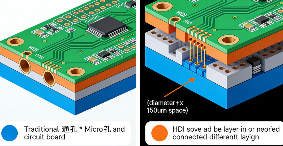
HDI PCBs are defined by their use of finer lines, micro-vias (blind, buried, and staggered), and higher connection pad density. This architecture fundamentally changes the design paradigm.
Micro-Vias and Layering: Unlike through-hole vias that penetrate the entire board, HDI utilizes micro-vias—laser-drilled holes with diameters typically less than 150 microns. These can be buried within layers or connect adjacent layers, freeing up vast amounts of surface and internal space. This allows designers to place components much closer together.

Increased Functionality per Square Inch: By utilizing both sides of the board more effectively and adding complex, dense interconnection layers, HDI PCBs can accommodate significantly more components in a smaller area. This is the direct technological driver behind ultra-thin smartphones, compact wearables, and powerful miniaturized medical devices.
The result is a dramatic reduction in overall product size and weight without sacrificing functionality—a key selling point for today's consumers.
Unlocking Superior Performance: The HDI Advantage
Beyond saving space, HDI PCB design delivers a substantial boost in performance and signal integrity, which is critical for high-speed applications.
Enhanced Signal Integrity: Shorter and more direct signal paths between components, enabled by micro-vias, reduce signal propagation delays and attenuation. This minimizes noise, cross-talk, and electromagnetic interference (EMI). For high-speed processors, memory, and RF components (like 5G/Bluetooth/Wi-Fi modules), this cleaner signal transmission is vital for stability and speed.
Improved Power Integrity: HDI designs facilitate better power distribution networks with optimized placement of decoupling capacitors and more efficient grounding. This ensures stable voltage delivery to sensitive components, preventing performance throttling and enhancing overall reliability.

Support for Advanced Components: Modern fine-pitch Ball Grid Array (BGA) and Chip-Scale Package (CSP) components require the dense pad layouts and micro-via technology that only HDI can provide. This allows integration of the latest, most powerful chipsets. Reliability and Design Flexibility
The advantages of HDI PCB design extend into product durability and development agility.
Increased Reliability: Fewer through-holes and more robust interconnect structures reduce the risk of failure under thermal or mechanical stress. The dense, compact layout also often leads to fewer solder joints and interconnects, which are potential points of failure.
Greater Design Freedom: Engineers are no longer as constrained by routing challenges. HDI technology allows for more creative and optimal component placement, enabling innovative product architectures and form factors that were previously impossible.
Applications Driving Demand
HDI PCBs are no longer a niche technology; they are the standard for cutting-edge consumer products:
Smartphones & Tablets: Enabling slimmer profiles, larger batteries, and advanced multi-camera systems.
Wearable Devices: Making compact, powerful smartwatches, fitness trackers, and AR/VR glasses feasible.
Ultrabooks & Convertibles: Supporting high-performance computing in razor-thin designs.
Advanced Consumer IoT: Powering miniaturized, connected sensors and smart home devices.
Conclusion: A Strategic Imperative for Innovation
For OEMs and designers aiming to lead the market, adopting HDI PCB technology is a strategic decision. It is the foundational enabler that reconciles the conflicting demands for miniaturization, enhanced performance, and increased functionality. The performance boost from HDI PCBs directly translates to faster, more responsive, and more reliable devices that capture consumer interest.
Ready to leverage HDI technology for your next breakthrough product? Partner with a PCB manufacturer that specializes in advanced HDI design and fabrication. Contact our team today to discuss how we can help you achieve technical upgrades and radical product miniaturization for a competitive advantage. If you have specific procurement intentions or need further assistance, please feel free to contact us at sales03@sunsoartech.com or call +8613632793113.


Comments