How to Prevent Common Soldering Defects in PCBA Processing: 7 Problems & Fixes
- afax TE.
- Dec 12, 2025
- 3 min read
Struggling with soldering defects? Learn how to prevent 7 common PCBA soldering issues like solder bridges & tombstoning. Get expert tips for reliable PCB assembly and solder joint inspection.
In the precise world of PCB Assembly (PCBA) processing, soldering quality is
paramount. Even minor soldering defects can lead to circuit failures, reduced reliability, and increased costs. Effective PCBA soldering defects prevention is not just a step; it’s a comprehensive strategy embedded in every stage of manufacturing. This guide explores seven frequent soldering problems, their root causes, and proven solutions to ensure robust, high-yield production.

Introduction to Soldering Quality
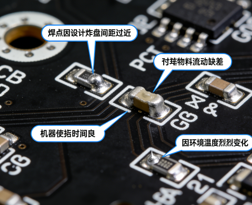
Soldering creates the essential electrical and mechanical connections on a PCB. Defects often stem from a combination of factors including design flaws, material issues, machine settings, and environmental conditions. Proactive prevention, backed by rigorous how to inspect PCB solder joints protocols, is key to excellence. Let’s delve into the common challenges.

7 Common PCBA Soldering Defects & How to Fix Them
1. Solder Bridges (Short Circuits)
Problem: Unintended connections of solder between two adjacent pins or pads, creating a short circuit.
Causes: Excessive solder paste, incorrect stencil design, poor component placement, or inadequate solder mask.
Solutions & Prevention:
Optimize stencil aperture design to control solder paste volume.
Ensure precise solder paste printing and clean stencil wiping.
Verify accurate component placement alignment.
Review PCB design to increase spacing between fine-pitch pads where possible.
2. Tombstoning (Manhattan Effect)
Problem: A passive component (like a resistor or capacitor) lifts vertically on one end, resembling a tombstone.
Causes: Imbalanced solder paste melting forces due to uneven pad sizing, asymmetrical thermal mass, or skewed placement.
Solutions & Prevention:
Design symmetrical pads with equal size and thermal connection.
Ensure precise, centered component placement.
Use a reflow profile with a controlled, even preheat stage to allow both ends to melt simultaneously. These are critical solder bridge and tombstoning fixes.
3. Insufficient Solder (Weak Joints)
Problem: Solder joints lack adequate solder, leading to poor electrical conductivity and mechanical strength.
Causes: Under-printed solder paste, poor wettability, or an overly aggressive reflow profile.
Solutions & Prevention:
Regularly calibrate and maintain the solder paste printer.
Use fresh, properly stored solder paste and ensure PCB surface finish is not oxidized.
Adjust reflow temperature and time to promote good wetting without burning the flux.
4. Solder Balls
Problem: Small spheres of solder scattered around pads or components after reflow.
Causes: Moisture absorption in solder paste, excessive paste slump, or contamination on the PCB surface.
Solutions & Prevention:
Follow strict handling and storage rules for solder paste (e.g., refrigeration, warm-up time).
Control workshop humidity.
Ensure the reflow profile has a proper preheat to gently evaporate solvents without spattering.
5. Voiding (in Solder Joints, especially BGA)
Problem: Air pockets or voids trapped within a solder joint, weakening thermal and electrical performance.
Causes: Outgassing from flux, moisture on pads or in paste, or an incorrect reflow profile.
Solutions & Prevention:
Use low-moisture, high-quality solder paste.
Bake PCBs and components if they are moisture-sensitive.
Optimize the reflow profile’s ramp-up rate and peak temperature to allow gases to escape.
6. Cold Solder Joints
Problem: A dull, grainy, and poorly connected joint that fails to properly fuse. It is a major reliability risk.
Causes: Insufficient heat during soldering, movement during cooling, or contaminated surfaces.
Solutions & Prevention:
Validate and monitor the reflow oven’s thermal profile across the board.
Ensure the conveyor is vibration-free.
Maintain clean, oxidation-free PCB and component surfaces. This is a vital part of PCBA soldering defects prevention.
7. Lifted Pads
Problem: The copper pad detaches from the PCB laminate, often taking the trace with it.
Causes: Excessive mechanical stress during manual soldering/desoldering, repeated thermal cycling, or poor PCB laminate quality.
Solutions & Prevention:
Train operators on proper manual soldering techniques (minimal force, correct temperature).
Use adequate thermal relief in PCB design for pads connected to large copper planes.
Source PCBs from reputable manufacturers with quality controls.
How to Inspect PCB Solder Joints for Defects
A robust inspection regimen catches defects early:
Visual Inspection (Manual/Microscope): Good for obvious bridges, tombstoning, or lifted pads.
Automated Optical Inspection (AOI): Uses cameras to quickly check for paste volume, placement, and post-reflow joint quality against a programmed standard.
X-Ray Inspection (AXI): Essential for hidden joints like those in BGA packages, revealing voids, bridges, and insufficient solder.
Electrical Testing (ICT/Flying Probe): Confirms electrical connectivity and function, catching defects that cause opens or shorts.

Conclusion
Preventing soldering defects in PCBA processing requires a holistic approach. It starts with a manufacturable design, continues with controlled material handling and precise machine operation, and is validated through systematic inspection. By understanding the root causes of these seven common problems and implementing the outlined solder bridge and tombstoning fixes and broader strategies, manufacturers can significantly improve yield, reliability, and customer satisfaction. If you have specific procurement intentions or need further assistance, please feel free to contact us at sales03@sunsoartech.com or call +8613632793113.


Comments